On NVIDIA GPUs from Volta onward, shared memory and the L1 cache occupy the same physical on-chip SRAM on each SM and have the same access latency, despite serving different programming roles. At kernel launch, the available SRAM can be partitioned between them. Earlier Maxwell- and Pascal-generation GPUs used separate SRAM pools. section 1.4
Figure 1.8 The memory hierarchy organized by speed and size. Registers top the hierarchy as the fastest and smallest storage; global memory sits at the bottom as the largest and slowest. Shared memory and the L1 cache appear on adjacent rows to reflect their distinct programming roles; on NVIDIA GPUs from the Volta architecture onwards, they share the same physical on-chip SRAM on each SM and have the same access latency, so the figure separates them by function, not by speed.
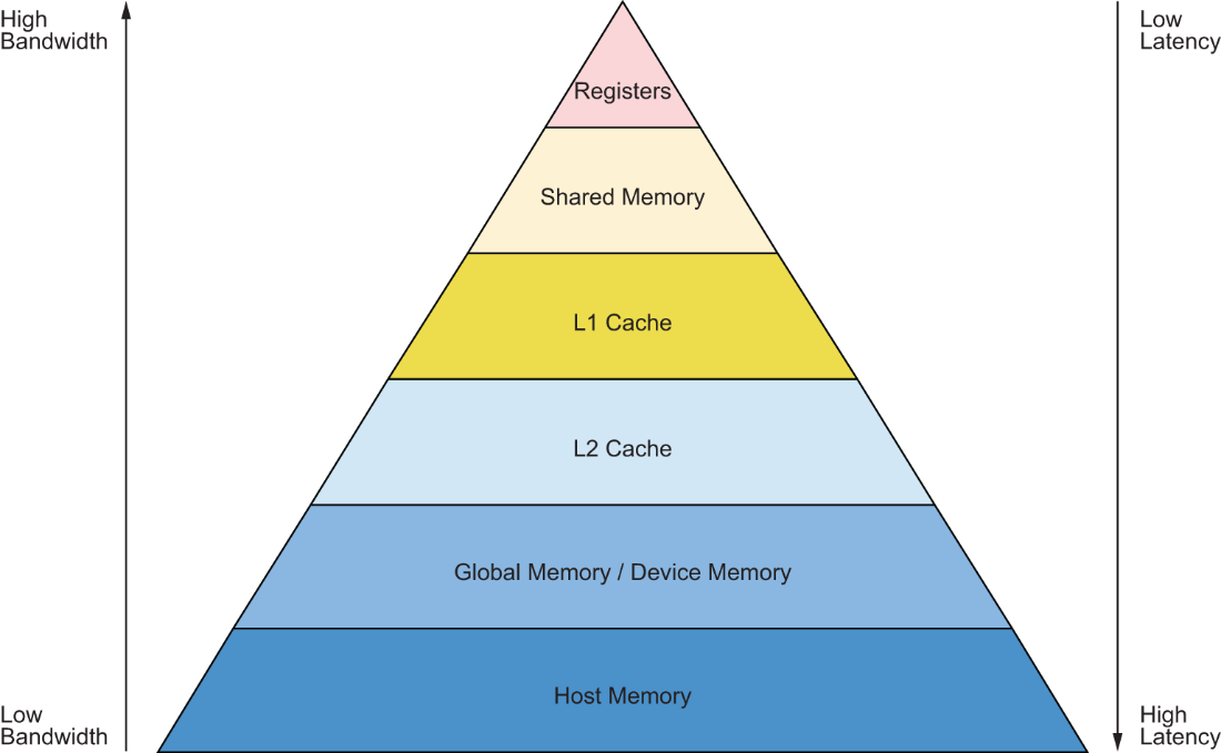
The memory-hierarchy diagram shows shared memory and L1 cache as distinct roles sharing SRAM on Volta-generation and later GPUs. section 1.4