DRAM stores each bit as charge on a capacitor, which must be refreshed periodically. Its one-transistor-per-bit cells provide more capacity per area than SRAM, at the cost of higher access latency. GPUs use DRAM for global memory, where large tensor and model storage matters more than the low latency of on-chip memory. section 1.4
Figure 1.8 The memory hierarchy organized by speed and size. Registers top the hierarchy as the fastest and smallest storage; global memory sits at the bottom as the largest and slowest. Shared memory and the L1 cache appear on adjacent rows to reflect their distinct programming roles; on NVIDIA GPUs from the Volta architecture onwards, they share the same physical on-chip SRAM on each SM and have the same access latency, so the figure separates them by function, not by speed.
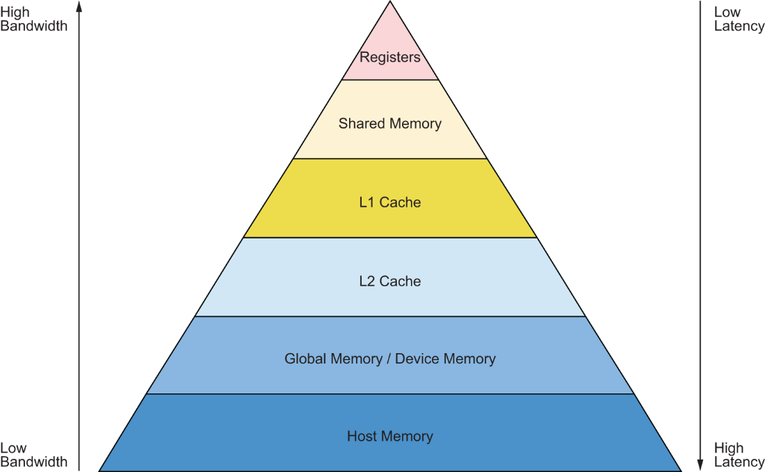
See where DRAM-based global memory sits in the GPU memory hierarchy relative to caches and registers. section 1.4