When a GPU kernel repeatedly accesses global memory, an L2 cache hit can supply data without another trip to DRAM. L2 is hardware-managed, so the programmer does not explicitly move data into it. It is generally larger and farther from the compute units than L1 cache. section 3.2.3 section 1.4
L1 is private to each streaming multiprocessor (SM), while L2 is shared across the GPU. L2 sits between the SMs and the memory controllers: global-memory reads and writes pass through it, as do host-device transfers over PCIe or NVLink. Its bandwidth can therefore matter alongside DRAM bandwidth. section 3.2.3
Figure 3.3 Memory system of an NVIDIA H100 GPU, showing per-SM register file, unified L1/shared memory, constant caches, the chip-level L2 cache, and HBM3 global memory (with PCIe/NVLink connectivity).
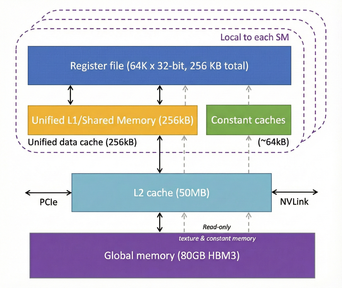
The H100 memory diagram places chip-wide L2 between the per-SM storage and HBM3 global memory. section 3.2
Cache reuse is one way to reduce expensive memory traffic; latency hiding is another. While some threads wait for data, the GPU can run other threads. Kernel scheduling choices can also encourage reuse: grouped program IDs in a matrix multiplication kernel encourage L2 reuse. section 1.4 section 5.10
H100 capacity and bandwidth
The NVIDIA H100 has roughly 50 MB of L2 cache and approximately 5.5 TB/s of L2 bandwidth. These figures are hardware-specific, not universal cache properties. section 3.2.3
Table 1.2 Measured memory access latency by hierarchy level, in GPU clock cycles, on Hopper-generation GPUs
| Memory level | Latency (cycles) |
Registers |
~1 |
Shared memory / L1 cache |
29 to 41 |
L2 cache |
258 to 744, since Hopper’s L2 is split into two partitions and the figure depends on which one a request hits and whether it is a hit or a miss |
Global memory (HBM) |
479 to 656 |
Hopper latency measurements show that L2 access costs vary with the partition accessed and whether the request hits or misses. section 1.4