A GPU can spend hundreds of clock cycles waiting for data from global memory. Its memory hierarchy places smaller, faster storage closer to computation and larger, slower storage farther away. Keeping frequently needed data near computation reduces trips to global memory and helps kernels use available bandwidth. section 1.4 section 3.2
Figure 1.8 The memory hierarchy organized by speed and size. Registers top the hierarchy as the fastest and smallest storage; global memory sits at the bottom as the largest and slowest. Shared memory and the L1 cache appear on adjacent rows to reflect their distinct programming roles; on NVIDIA GPUs from the Volta architecture onwards, they share the same physical on-chip SRAM on each SM and have the same access latency, so the figure separates them by function, not by speed.
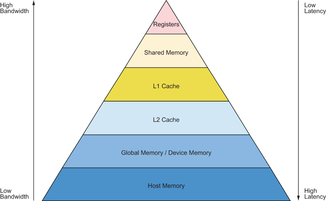
The pyramid orders the five levels by size and speed, with shared memory and L1 distinguished by their programming roles. section 1.4
From the smallest and fastest end of the hierarchy:
- Registers are private to each thread and hold active operands and results for arithmetic. section 1.4
- Shared memory and L1 cache serve different programming roles. On NVIDIA Volta and later GPUs, they occupy the same on-chip SRAM on each streaming multiprocessor (SM) and have the same access latency. section 1.4
- L2 cache sits between the on-chip levels and global memory. On the NVIDIA H100, it is shared at the chip level. section 1.4 section 3.2
- Global memory provides the largest, slowest tier. The H100 uses HBM3 for global memory. section 1.4 section 3.2
The hierarchy works alongside latency hiding: while some threads wait for memory, other ready threads compute. Efficient kernels still need to make good use of bandwidth; concurrency alone does not remove the cost of moving data. section 1.4 section 3.2
Table 1.2 Measured memory access latency by hierarchy level, in GPU clock cycles, on Hopper-generation GPUs
| Memory level | Latency (cycles) |
Registers |
~1 |
Shared memory / L1 cache |
29 to 41 |
L2 cache |
258 to 744, since Hopper’s L2 is split into two partitions and the figure depends on which one a request hits and whether it is a hit or a miss |
Global memory (HBM) |
479 to 656 |
Measured Hopper latencies illustrate the scale of the differences. The reported L2 range depends on the partition and whether the request hits or misses, so measured ranges need not be strictly ordered. section 1.4
Inspect the target GPU
For a GPU you use, identify its model, architecture, SM count, memory type and capacity, and peak memory bandwidth. Compare these specifications with the H100 rather than assuming its characteristics apply to your device. section 3.6.1 section 3.2